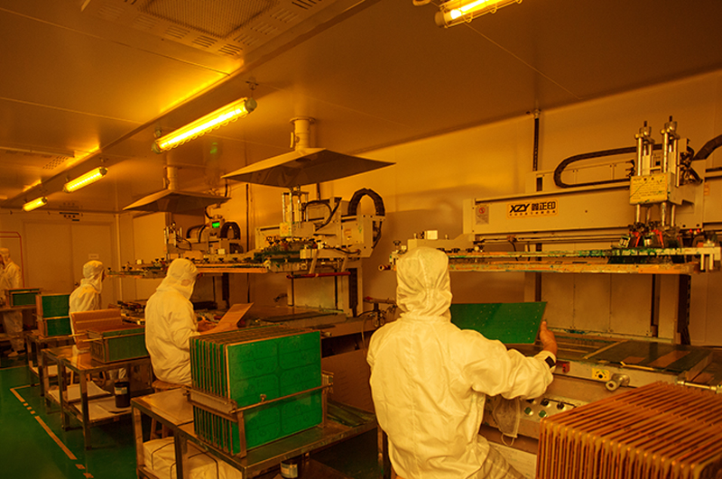
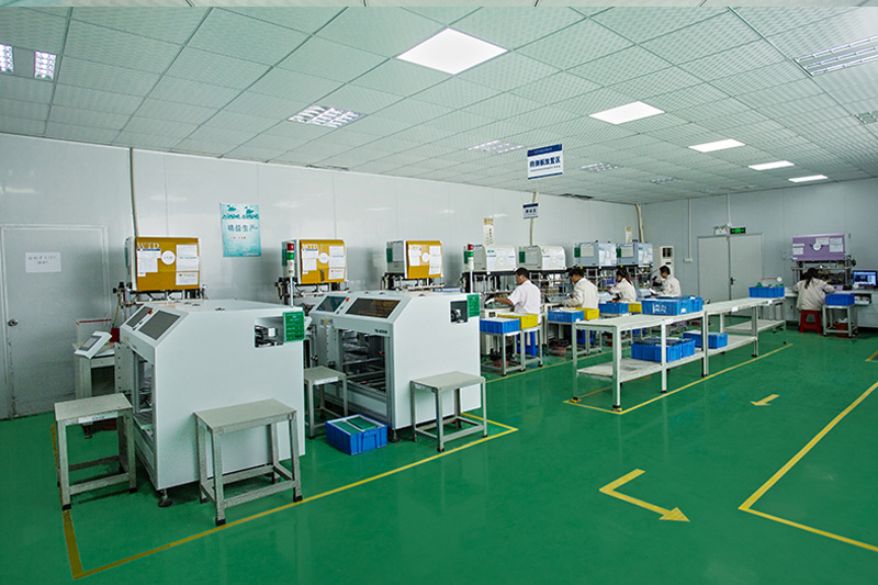
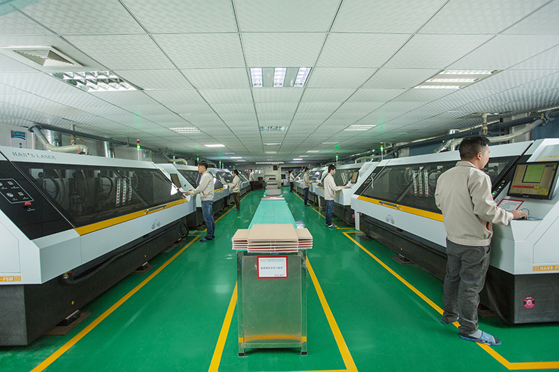
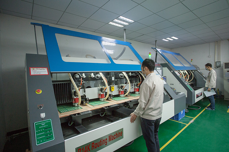
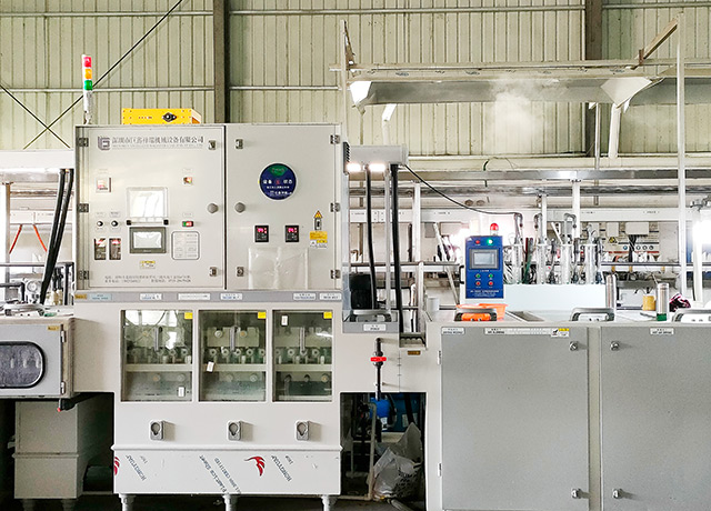
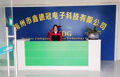
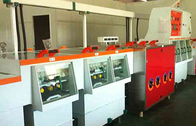
Company profile
PCB circuit board is the support of electronic components and the provider of electrical connection of electronic components. According to the number of circuit layers, it can be divided into single panel, double-sided board and multilayer board. The common multilayer board is generally 4-layer board or 6-layer board, and the complex multilayer board can reach more than ten layers. So, here's a brief introduction
Metal half hole (groove) refers to the second drilling and shape process after the first drilling hole is perforated, and finally the metallized hole is retained (slot) half, that is, the metallized hole on the board edge is cut in half. In the PCB industry, it is also called stamp hole. The hole edge can be directly welded with the main edge to save connector and space. It often appears in the signal circuit. What is the production process flow of half hole PCB?
The production of PCB is not difficult, but the difficulty lies in the troubleshooting after production. So, what are the methods to find PCB faults?Common PCB circuit board faults mainly focus on components, such as capacitors, resistors, inductors, diodes, triodes, field effect tubes, etc., and obvious damage to integrated chips and crystal oscillators.
The number of layers of PCB depends on the complexity of the circuit board. PCB stack design is an important part of PCB design, which directly affects the quality of PCB finished products. So, what are the general rules of PCB stack design?
With the rapid development of electronic components, power circuit board PCB design is facing greater challenges, mainly including power conversion efficiency, thermal analysis, power plane integrity and EMI (electromagnetic interference). What are the common problems in PCB design of power circuit board?