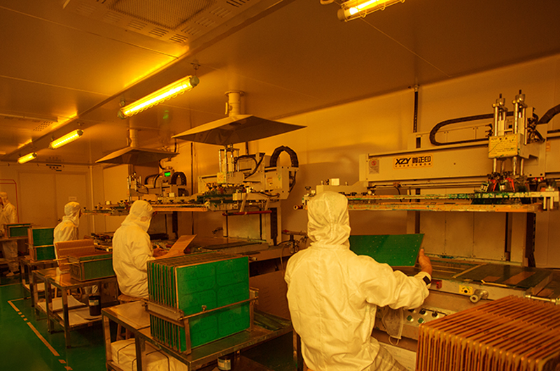
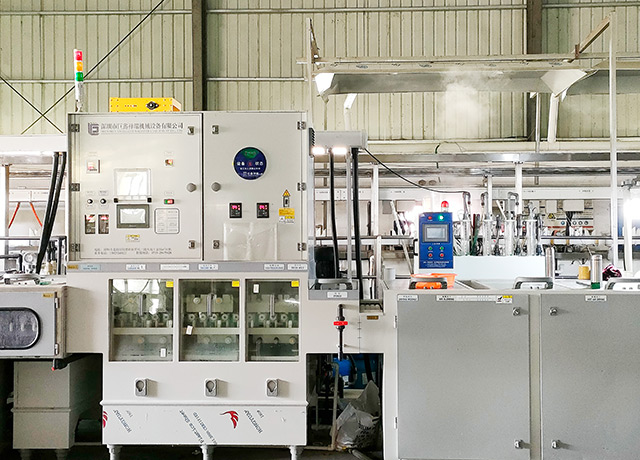
PCB circuit board is the support of electronic components and the provider of electrical connection of electronic components. According to the number of circuit layers, it can be divided into single panel, double-sided board and multilayer board. The common multilayer board is generally 4-layer board or 6-layer board, and the complex multilayer board can reach more than ten layers. So, here's a brief introduction
Metal half hole (groove) refers to the second drilling and shape process after the first drilling hole is perforated, and finally the metallized hole is retained (slot) half, that is, the metallized hole on the board edge is cut in half. In the PCB industry, it is also called stamp hole. The hole edge can be directly welded with the main edge to save connector and space. It often appears in the signal circuit. What is the production process flow of half hole PCB?
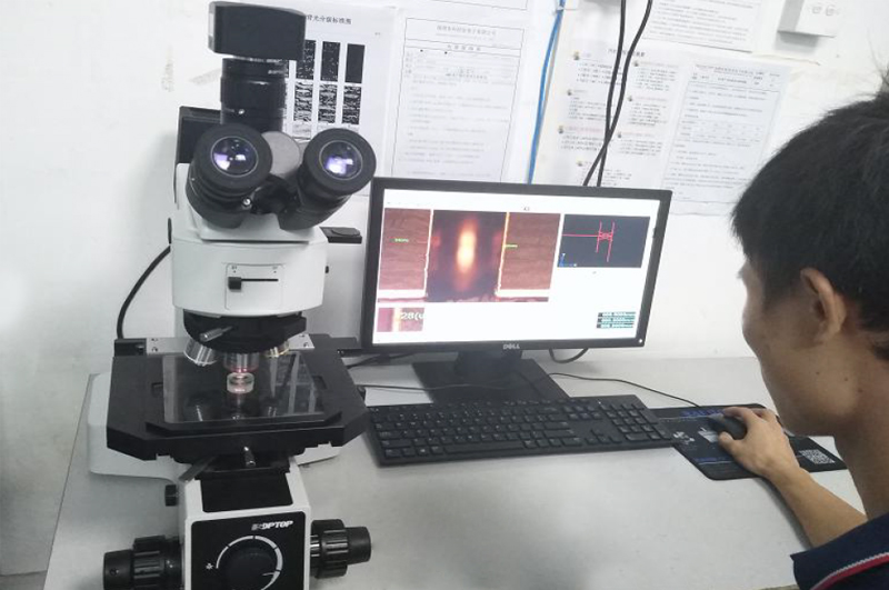
The production of PCB is not difficult, but the difficulty lies in the troubleshooting after production. So, what are the methods to find PCB faults?Common PCB circuit board faults mainly focus on components, such as capacitors, resistors, inductors, diodes, triodes, field effect tubes, etc., and obvious damage to integrated chips and crystal oscillators.
The number of layers of PCB depends on the complexity of the circuit board. PCB stack design is an important part of PCB design, which directly affects the quality of PCB finished products. So, what are the general rules of PCB stack design?
With the rapid development of electronic components, power circuit board PCB design is facing greater challenges, mainly including power conversion efficiency, thermal analysis, power plane integrity and EMI (electromagnetic interference). What are the common problems in PCB design of power circuit board?
Different point settings are required in different stages of design, and large grid points can be used for device layout in the layout stage;
For large devices such as IC and non positioning connectors, the grid precision of 50 ~ 100mil can be used for layout, while for passive small devices such as resistance, capacitance and inductance, the grid precision of 25mil can be used for layout. The accuracy of large grid points is conducive to the alignment and beautiful layout of devices.
Consumer electronics is mainly concentrated in mobile phones, TVs, PCs and other fields, while in the field of smart phones with the highest proportion of downstream terminals, China's sales volume significantly exceeds that of the United States.
The scale of China's smartphone market has continued to grow rapidly in recent years, far exceeding the average single digit growth level of the industry, which is inseparable from the improvement of China's huge population base, rapidly developing electronic supporting industry chain, communication base station and other infrastructure.
1. If the designed circuit system contains FPGA devices, the pin assignment must be verified by Quartus II software before drawing the schematic diagram. (some special pins in FPGA cannot be used as ordinary IO).
Printed circuit board is the most active industry in the contemporary electronic component industry, and its industry growth rate is generally about 3 percentage points higher than that of the electronic component industry. It is expected to maintain rapid growth in 2006. Demand upgrading and industrial transfer are the basic driving forces to promote the development of the industry, and HDI board, flexible board, IC packaging board (BGA, CSP) and other varieties will become the main growth points.